
AI-Innovationen in der Materialwissenschaft: Atomare Defekte zerstörungsfrei aufdecken
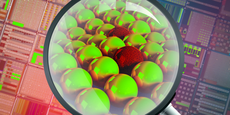
In der Biologie werden Defekte normalerweise als Probleme angesehen. Aber in der Materialwissenschaft wird das Drehbuch umgedreht: Defekte werden manipuliert und kontrolliert, um den Materialien die gewünschten Eigenschaften zu verleihen. Dabei handelt es sich nicht um einen zerstörerischen Prozess, sondern um einen sorgfältigen Ansatz, der in der modernen Fertigung eingesetzt wird. Denken Sie an Produkte wie Stahl, Halbleiter oder Solarzellen, bei denen Defekte auf atomarer Ebene mit Präzision eingebracht werden, um die Leistung zu erhöhen, die elektrische Leitfähigkeit zu regulieren, die Leistung zu optimieren und vieles mehr. Doch so viele Vorteile kontrollierte Defekte auch mit sich bringen, ihre Messung ist nach wie vor knifflig. Wie Wissenschaftler herausgefunden haben, gibt es keine einfache Möglichkeit, verschiedene Defektarten und -konzentrationen zu visualisieren und zu quantifizieren, ohne die Integrität des Endprodukts zu beeinträchtigen.
AI's neues Projekt in der Defekterkennung
Mit dem Aufkommen der künstlichen Intelligenz könnte sich dies ändern. Forscher am MIT haben künstliche Intelligenz auf eine neue Weise eingesetzt und ein KI-Modell entwickelt, das in der Lage ist, bestimmte Defekte zu klassifizieren und zu quantifizieren. Ihre Methode ist nicht invasiv und nutzt Daten aus der Neutronenstreuung. Nachdem das Modell mit 2 000 verschiedenen Halbleitermaterialien trainiert wurde, ist es nun in der Lage, bis zu sechs Arten von Punktdefekten gleichzeitig zu erkennen. Herkömmliche Techniken hätten Mühe, dieselben Ergebnisse zu erzielen. “Bestehende Techniken können Defekte nicht universell und quantitativ genau charakterisieren, ohne das Material zu zerstören”, sagt Mouyang Cheng, Doktorand am MIT Department of Materials Science and Engineering.
Man hofft, dass dieses innovative KI-Modell den Bereich der Fehlererkennung effektiv voranbringen kann. Wenn wir Defekte besser verstehen, können wir Materialien noch nützlicher machen. Mingda Li, Hauptautorin der Forschungsarbeit, verglich die herkömmlichen Methoden zur Fehlererkennung mit der eingeschränkten Perspektive, die man bei der Beobachtung eines Elefanten hat: Jeder kann nur einen Teil sehen, aber nicht das Ganze. “Wir brauchen bessere Methoden, um uns ein vollständiges Bild von Defekten zu machen, denn wir müssen sie verstehen, um die Materialien nützlicher zu machen”, betonte Li.
Reise über konventionelle Grenzen hinaus
Zu diesem Zeitpunkt können die Hersteller zwar Fehler einführen, haben aber immer noch Schwierigkeiten, deren Auswirkungen auf die fertigen Produkte genau zu messen. Herkömmliche, invasive Tests sind eine langsame, wenig effektive Lösung. Die vom MIT-Team entwickelte KI-Lösung ist zwar auf ihre Weise perfekt, könnte aber für viele Branchen anfängliche Integrationsprobleme mit sich bringen. Es handelt sich um eine Technik, die auf komplizierten, mit Neutronen gemessenen Schwingungsfrequenzen basiert. Obwohl die Methode unbestreitbar sehr leistungsfähig ist, ist sie nicht ohne Weiteres verfügbar. Die Forscher sind jedoch davon überzeugt, dass ihre Studie den Grundstein für die Zukunft der Defektforschung legen kann.
Für die Zukunft plant das Team, ein ähnliches Modell auf der Grundlage von Raman-Spektroskopiedaten zu trainieren. Unternehmen haben bereits Interesse an dieser Technik gezeigt, bei der es sich um ein weit verbreitetes Verfahren zur Messung der Dispersion von Licht handelt. Im Zuge der weiteren Arbeit hofft das Team auch, den Funktionshorizont seines Werkzeugs zu erweitern und mehr als nur Punktdefekte zu erkennen. Zu diesem Zweck haben sie derzeit Defekte wie Körner und Versetzungen auf dem Radar.
Mit KI die Zukunft gestalten
Die Fähigkeit der künstlichen Intelligenz, verschiedene Signale zu erkennen und die Grundwahrheit zu enthüllen, ist sowohl spannend als auch vielversprechend. “Defekte sind ein zweischneidiges Schwert. Es gibt viele gute Defekte, aber wenn es zu viele sind, kann die Leistung sinken. Damit eröffnet sich ein neues Paradigma in der Defektforschung”, so Li. Ihre Arbeit, die zum Teil vom US-Energieministerium und der National Science Foundation unterstützt wird, zeigt uns, wie KI die Zukunft der Defektforschung und der Materialherstellung gestalten kann.
Da sich KI weiterentwickelt und sich auf verschiedene Bereiche auswirkt, erforschen Unternehmen weltweit Automatisierungslösungen. Wenn Sie das Gleiche für Ihr Unternehmen planen, sollten Sie sich implementi.ai ansehen. Es könnte genau das sein, was Sie brauchen, um Ihre Geschäftsprozesse zu revolutionieren. Ergreifen Sie die Initiative und gestalten Sie Ihre Zukunft mit KI.


